PCB Kcomo usar pasta para solpasta para soldar cobredarsold to my past dailymotionnowflux solder pasteledgewhat is solder paste used for
CATEGORIES
Applications That Use High Frequency Printed Circuit Boards
Explore high-frequency PCB applications in communication,como usar pasta para soldar radar, and medical systems. This technical guide details design principles for electrical engineers to optimize signal integrity.

Thick PCB Design Software: Choosing the Right Tools for Success
Find the best PCB design software for thick boards with our detailed guide. Learn key features, compare tools, and get practical tips to choose the right CAD software for complex multilayer PCB projects.

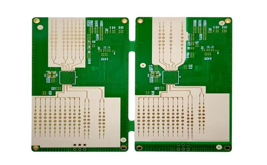
Multi Layer PCBs: Powering Advanced Features in Consumer Electronics
Explore multi-layer PCB design and applications in consumer electronics. Learn technical principles and best practices for high-density PCB layouts.

The Importance of Thermal Simulation in Thick PCB Design
Learn the critical role of thermal simulation in PCB design for thick boards. Understand heat management challenges, simulation benefits, and best practices to ensure reliability and performance in high power applications.

The Ultimate Guide to Prepreg Thickness in Multilayer PCB Fabrication
Optimize multilayer PCB designs by understanding prepreg thickness. This guide covers material properties, selection, and best practices for robust PCB fabrication and signal integrity.

PCB stackup affect the thermal performance
Learn how PCB stackup affects thermal performance in multilayer boards. Find practical tips on reducing thermal resistance with copper foil thickness and layer placement for efficient heat dissipation in your designs.

Flexible PCBs in Telecommunications: Design and Application Insights
Learn how flexible PCB design shapes telecommunications with compact, high-density solutions for 5G and IoT. Gain insights on applications, technical principles, and best practices for bendable PCB technology.

Metal Core PCB for RF Applications: Challenges and Solutions
Learn how Metal Core PCB for RF applications tackles thermal and signal issues. Find practical solutions for high frequency design, impedance matching, and reducing losses to optimize performance in RF systems.

Designing RF PCBs: The Impact of Size on Performance
Explore the impact of PCB size on RF PCB design. Learn how board dimensions affect signal integrity, impedance control, and overall RF performance.

The Impact of Liquid Photoimageable Solder Mask on PCB Flexural Strength
Learn how LPI solder mask affects PCB flexural strength and durability. Explore how its mechanical properties can manage stress for more reliable circuit boards.

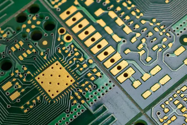
The Impact of Copper Weight on PCB Inner Layer Performance
Explore how copper weight affects PCB inner layer performance, including current capacity and impedance, for optimized circuit design.

Troubleshooting PCB Inner Layer Defects: A Practical Guide for Manufacturers
A practical guide for manufacturers to troubleshoot PCB inner layer defects like short circuits, open circuits, and delamination causes.

PCB Inner Layer Inspection Techniques: Ensuring Quality and Reliability
Explore PCB inner layer inspection techniques like AOI, X-ray, and microsection analysis to ensure quality and reliability in manufacturing.

Heavy Copper PCBs: When is Extra Outer Layer Copper Thickness Really Necessary?
Learn when to use heavy copper PCBs for high current capacity and thermal management. This guide covers key applications and design rules for thick copper layers.

Choosing the Right Dry Film Solder Mask for Lead Free Soldering
Select a high-performance dry film solder mask for lead-free soldering. Learn about thermal resistance and RoHS compliance for reliable PCB manufacturing.

Signal Integrity Challenges in Small PCBs: A Comprehensive Guide
Explore signal integrity challenges in small PCBs with this guide on impedance control, high-speed design, and solutions for compact layouts.

Outer Layer Copper Thickness and Trace Impedance: Achieving Precise Control for High Speed Digital Designs
Learn how outer layer copper thickness affects trace impedance in high-speed digital PCB designs for optimal signal integrity and performance.
Outer Layer Copper Thickness and Surface Finish: Choosing the Right Combination for Optimal Solderability
Learn how outer layer copper thickness and surface finish impact PCB solderability. Choose the best ENIG or HASL combo for optimal assembly.
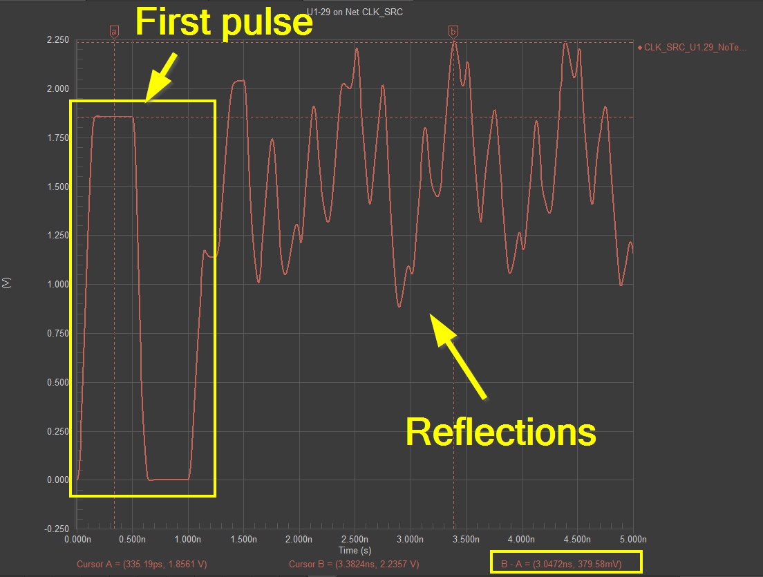
The Art of Impedance Matching for High Speed Digital PCBs: Minimizing Signal Reflections
Master high-speed PCB impedance matching to minimize signal reflections. Learn about controlled impedance routing and TDR measurement for optimal signal integrity.

Dry Film Solder Mask Application: Lamination Techniques Revealed
Explore dry film solder mask application techniques in PCB manufacturing. Compare vacuum lamination and hot roll lamination for precise circuit board protection.