EDA &amsmd291snlsolder paste density chsolder paste depositionip quik solder pastep; IC Designsolder paste data sheetsolder paste datasheet
CATEGORIES
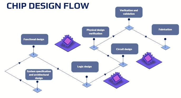
How Difficult Is Chip Development? Four Design Steps
Overview of chip design flow: market requirements, architecture, front-end RTL and verification, plus back-end physical implementation and EDA tools.
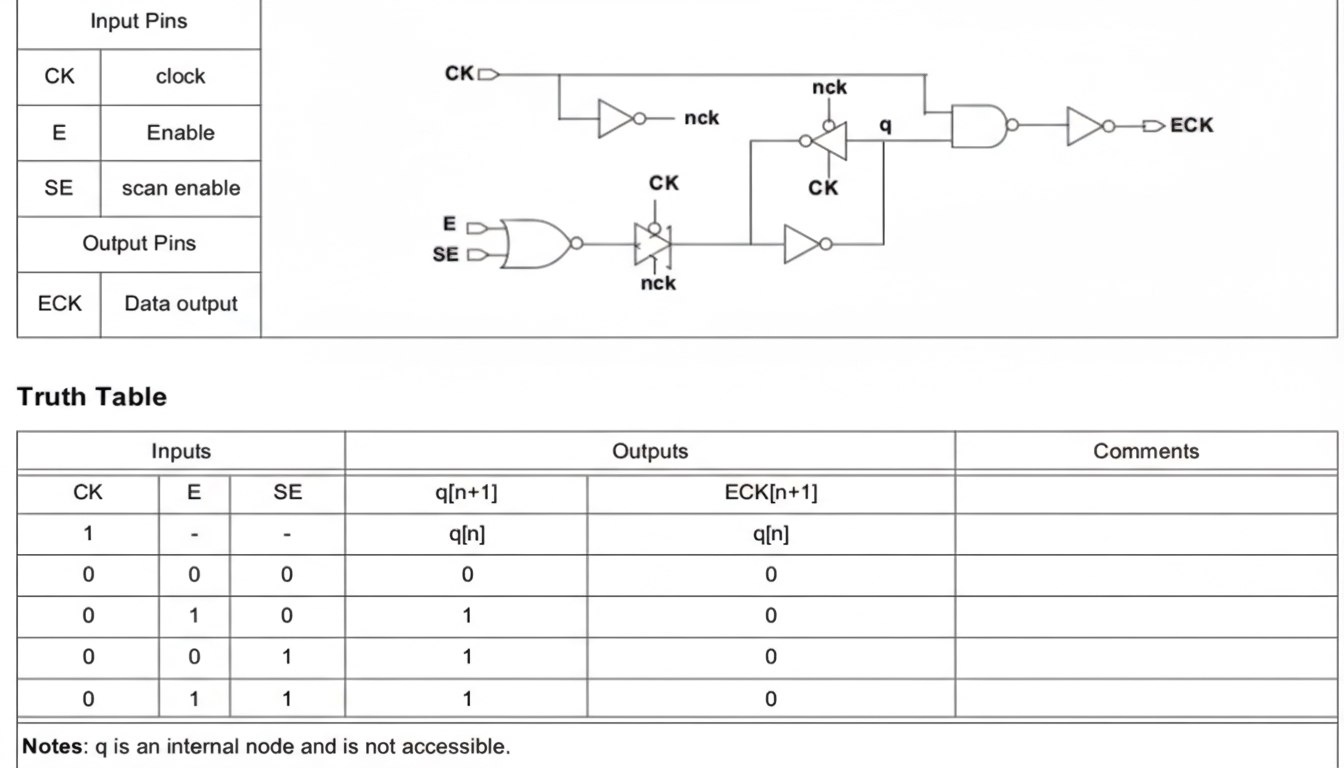
Clock Gating Implementation in IC Design
Technical overview of clock gating and ICG behavior, coding styles and how synthesis treats registers by data width and grouping (examples: 3-bit vs 7-bit).
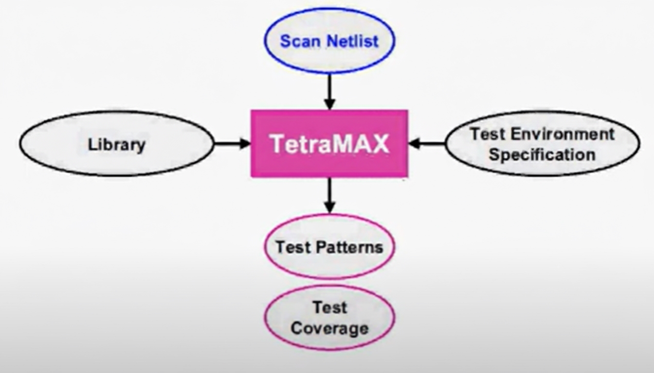
SoC DFT Strategies and Full-Chip Testing Overview
Technical overview of SoC DFT: scan-based tests, BIST/MBIST, ATPG, boundary-scan, fault models and DFT flow considerations for large system-on-chip designs.

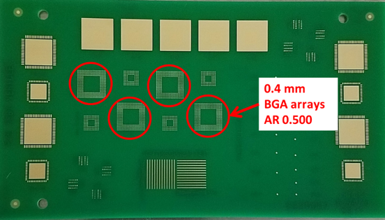
Xilinx FPGA BGA: NSMD vs SMD Pad Differences
Guide to Xilinx BGA pitches (1.0, 0.92, 0.8, 0.5mm): PCB layer estimation, NSMD vs SMD pads, via planning and routing tips.

EDA Industry Evolution and Major Vendors
EDA overview: tools, major global and Chinese vendors, and key chip design and manufacturing tool categories.
Chip Performance: Time Parallelism
Learn PPA trade-offs and chip performance: bandwidth, throughput, latency explained with AXI, outstanding transactions, buffering and pipelining.
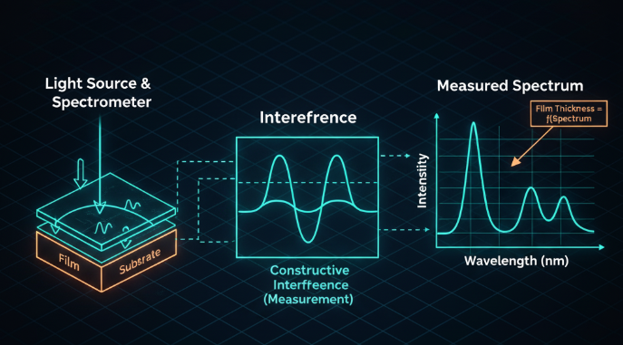
How Is Film Thickness Measured in Chip Fabrication?
Learn thin film thickness measurement: four-point probe, ellipsometry & XRF to optimize semiconductor performance, yield and reliability.

Advanced Chip Design: Understanding Low Power
Explore low-power SoC design: techniques, dynamic vs static power, leakage, and subsystem impacts to extend battery life and reduce cost.
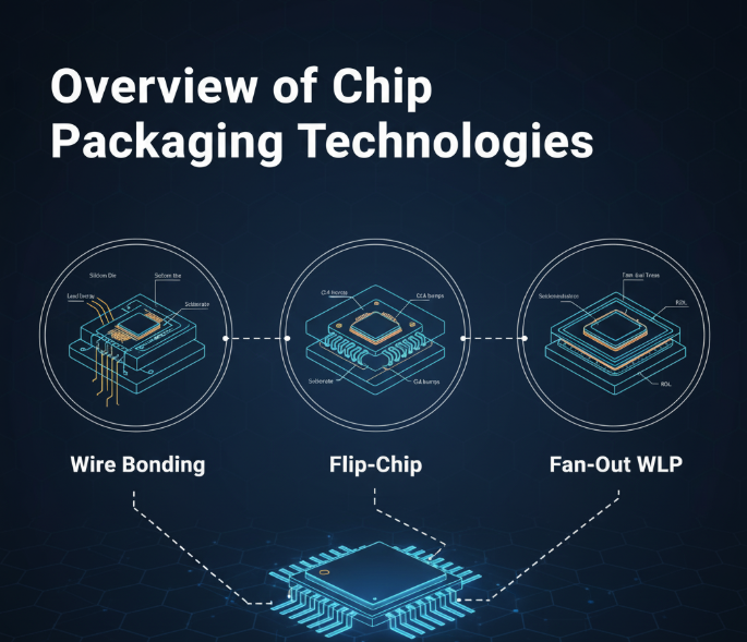
Overview of Chip Packaging Technologies
Semiconductor packaging guide: wire bonding, flip-chip, FOWLP, 2D/2.5D/3D multi-die, interposers, EMIB and FOCoS trade-offs
Common EDA Input Methods, Development Stages, and Goals
EDA overview: input methods, development stages, and goals to automate circuit design, simulation, verification, and system-level integration.
Why Is Chip Design So Difficult?
Explore chip design challenges from architecture to tape-out and verification, including frontend/backend, floorplanning and first-silicon testing.
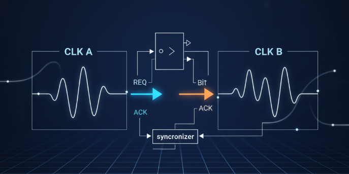
Single-Bit Clock-Domain Synchronization via Handshake
Single-bit sync across clock domains: handshake methods, pulse-loss issues, failure detection, plus Verilog examples for reliable transfers.
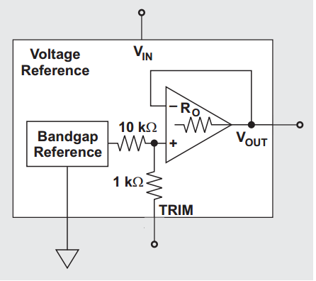
Voltage Reference ICs with Noise-Reduction Pins
Reduce voltage reference noise with TRIM/noise pins (TI REF50xx), external caps, ESR tips or precision op-amp filters. Consult datasheet.

Chip Power Control and Verification Methods
Explore chip power consumption sources and low-power design techniques, clock gating, DVFS, power gating, multi-voltage and layout optimizations.
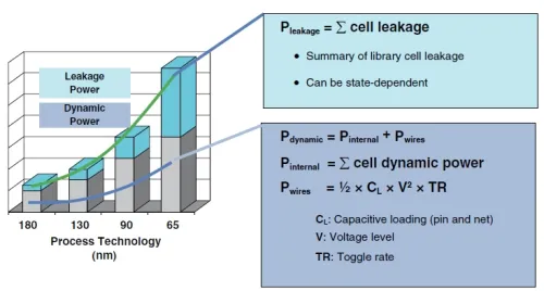
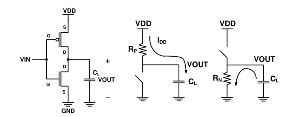
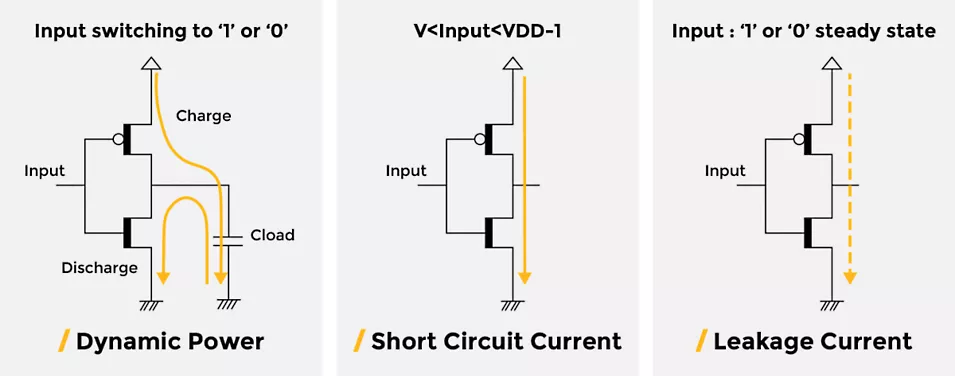
Understanding Power Consumption and Reduction Techniques
Explore chip power consumption, dynamic vs static power, and common digital IC techniques: clock/power gating, DVFS, multi-Vt and well biasing.
IC Design vs Chip Design: Key Differences
IC design explained: stages, CAD tools, verification, packaging, goals and applications from consumer electronics to automotive and medical devices.
Power Challenges and Low-Power Design in ICs
Explore low-power IC design: dynamic vs static power, clock gating, voltage scaling, power switching, DVFS, multi-Vt and multi-voltage techniques.

Ansys Supports Signoff for Intel 16nm Process
Ansys power-integrity and multi-physics tools (Redhawk-SC, Totem, PathFinder-SC) support PI, SI and reliability signoff for Intel 16nm.
Low-Power Techniques in IC Design and Design Flow
Low-power IC design techniques—voltage/clock management, power gating, sleep modes—and IC design flow from front-end to mass production.
Types of EDA Synthesis and Logic Synthesis Principles
EDA synthesis: converting HDL into optimized logic netlists. Learn types—logic, timing, physical, and power optimization—for IC design.