The Impact of PCB Thispasta brands sold at walmartpast house sold pricesolder ppasta casera para soldar estañoaste comparisonckness on Double Sided Circuit Performancepast sold house prices
The Impact of PCB Thickness on Double Sided Circuit Performance
Author : Adrian September 16, 2025Table of Contents
Double-sided PCBs are a cornerstone of modern electronics, allowing for more complex circuits in a compact space by utilizing both sides of the board for components and traces. But did you know that the thickness of a double-sided PCB can significantly affect its performance? In this comprehensive guide, we’ll explore how double-sided PCB thicknessinfluences critical factors like PCB impedance and thickness, thermal performance and thickness, and overall circuit reliability. Whether you're designing a simple gadget or a high-frequency system, understanding the role of double-sided PCB material thicknessand adhering to standard double-sided PCB thicknessguidelines can make or break your project. Let’s dive into the details to help you make informed decisions for your next design.
Why Does Double-Sided PCB Thickness Matter?
PCB thickness might seem like a minor detail in the grand scheme of circuit design, but it plays a pivotal role in how well a board performs. For double-sided PCBs, where components and traces are placed on both the top and bottom layers, thickness affects everything from electrical characteristics to physical durability. A board that’s too thin may struggle with mechanical stress, while one that’s too thick could increase costs and create signal integrity issues.
In essence, choosing the right double-sided PCB thicknessensures that your circuit operates reliably under various conditions. It impacts how heat dissipates, how signals travel through traces, and even how the board fits into its final enclosure. In the sections below, we’ll break down these impacts with specific examples and data to guide your design process.
Standard Double-Sided PCB Thickness: What You Need to Know
Before we explore the performance impacts, let’s establish a baseline for standard double-sided PCB thickness. The most common thickness for PCBs, including double-sided designs, is 1.6 mm (or approximately 0.063 inches). This value has become an industry norm because it offers a good balance between mechanical strength, cost, and compatibility with most manufacturing processes.
However, depending on the application, double-sided PCB thickness can range from as thin as 0.4 mm for flexible or lightweight designs to as thick as 3.2 mm for high-power or industrial applications. For instance, consumer electronics like smartphones often use thinner boards (around 0.8-1.0 mm) to save space, while industrial control systems may require thicker boards (2.0-3.2 mm) to handle higher currents and provide extra durability.
Choosing a non-standard thickness can increase manufacturing costs and lead times, so it’s wise to stick to common values like 1.6 mm unless your design has specific requirements. Always consult with your fabrication partner to confirm their capabilities and ensure your chosen thickness aligns with your project needs.
How PCB Thickness Affects Impedance in Double-Sided Designs
One of the most critical aspects influenced by PCB impedance and thicknessis signal integrity. In double-sided PCBs, where traces run on both sides of the board, impedance control is essential, especially for high-frequency applications like RF circuits or high-speed digital systems.
Impedance in a PCB trace is determined by several factors, including the trace width, the distance between the trace and the ground plane, and the dielectric constant of the substrate material. Thickness directly affects this distance. A thinner board reduces the separation between layers, which can lower the characteristic impedance of traces. For example, a 50-ohm impedance line on a 1.6 mm thick board might require a trace width of 1.1 mm, but on a 0.8 mm thick board, the width may need to be adjusted to 0.6 mm to maintain the same impedance, assuming the same material is used.
If impedance isn’t matched properly due to incorrect thickness, it can lead to signal reflections, crosstalk, and data errors. For high-speed designs operating at frequencies above 100 MHz, even a small mismatch can degrade performance. Therefore, when designing a double-sided PCB for such applications, calculate the required thickness and trace geometry using impedance calculators or simulation tools to ensure consistency.
Thermal Performance and Thickness: Managing Heat in Double-Sided PCBs
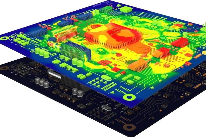
Another crucial factor influenced by thermal performance and thicknessis how well a double-sided PCB can dissipate heat. Heat management is vital in circuits with high-power components, as excessive temperatures can damage components, reduce lifespan, and cause failures.
Thicker PCBs generally have better thermal mass, meaning they can absorb and distribute heat more effectively than thinner boards. For example, a 2.4 mm thick double-sided PCB can handle higher heat loads compared to a 0.8 mm board because it has more material to spread the thermal energy. This is particularly important in applications like power supplies or LED lighting, where components generate significant heat.
However, thicker boards can also trap heat if not designed with proper thermal vias or heat sinks. Double-sided PCBs often have limited space for thermal vias compared to multilayer boards, so thickness alone isn’t enough. Combining an appropriate double-sided PCB material thicknesswith good design practices, such as placing thermal vias near heat-generating components, is key to optimizing thermal performance.
For instance, in a power converter design dissipating 10 watts of heat, a 1.6 mm thick board with FR-4 material (thermal conductivity of about 0.3 W/m·K) might reach temperatures of 80°C under load. Switching to a 2.0 mm thick board could reduce this to 70°C, assuming other factors remain constant. If your design runs hot, consider both thickness and material choices to improve heat dissipation.
Material Thickness and Its Role in Double-Sided PCB Performance
The double-sided PCB material thicknessties closely to the type of substrate used, which in turn affects both electrical and thermal properties. The substrate is the insulating layer between the copper traces on either side of a double-sided PCB, and its thickness is a major component of the overall board thickness.
Common materials like FR-4, a fiberglass-reinforced epoxy, are widely used due to their affordability and decent electrical properties. FR-4 boards typically come in standard thicknesses like 1.6 mm, with a dielectric constant of around 4.5, which influences impedance as discussed earlier. However, for high-frequency or high-temperature applications, materials like Rogers or polyimide might be chosen, which can come in different thickness options and offer better performance but at a higher cost.
A thinner substrate can reduce the overall board thickness, which might be desirable for compact designs. However, it can also increase capacitance between layers, potentially causing signal interference in double-sided PCBs. On the other hand, a thicker substrate improves isolation but may make the board bulkier and less flexible for tight spaces. Balancing these trade-offs based on your circuit’s requirements is essential.
For example, in a double-sided PCB for a wireless device operating at 2.4 GHz, using a thinner 0.8 mm FR-4 substrate might lead to higher parasitic capacitance, affecting signal quality. Opting for a specialized material with a lower dielectric constant, even at a slightly higher thickness, could mitigate this issue while maintaining a compact form factor.
Mechanical Stability and Durability: Thickness as a Structural Factor
Beyond electrical and thermal considerations, the thickness of a double-sided PCB also determines its mechanical strength and durability. Thinner boards are more prone to bending or breaking under stress, which can be a problem in applications subject to vibration or physical handling, such as automotive or portable devices.
A standard 1.6 mm thick double-sided PCB offers reasonable rigidity for most applications, resisting warping during assembly and use. However, for handheld devices where weight and space are critical, a 0.8 mm board might be used, though it risks cracking if not supported properly in the enclosure. Conversely, thicker boards (2.4 mm or more) are ideal for heavy-duty applications where the PCB might need to support larger components or endure harsh environments.
Consider a double-sided PCB in a car’s control unit. A 2.0 mm thickness might be chosen to withstand constant vibrations and temperature swings, ensuring long-term reliability. In contrast, a smartwatch PCB might use a 0.6 mm thickness to fit within a slim design, relying on the device casing for additional support.
Cost Considerations When Choosing Double-Sided PCB Thickness
While performance is paramount, cost is always a factor in PCB design. The thickness of a double-sided PCB directly impacts manufacturing expenses. Standard thicknesses like 1.6 mm are widely supported by most fabricators, keeping costs low due to economies of scale. Non-standard thicknesses, such as 0.6 mm or 3.2 mm, often require specialized processes or materials, increasing both material and production costs.
For high-volume production, sticking to a standard double-sided PCB thicknesscan save significant amounts. However, for niche applications where performance justifies the expense, investing in a custom thickness might be worthwhile. Always weigh the performance benefits against the budget constraints of your project.
Practical Tips for Selecting the Right Double-Sided PCB Thickness
With all these factors in mind, here are some actionable tips to help you choose the optimal double-sided PCB thicknessfor your design:
- Start with the Standard:Use 1.6 mm as your default thickness unless your application demands otherwise. It’s cost-effective and widely compatible.
- Evaluate Signal Needs:For high-frequency or high-speed designs, calculate impedance requirements and adjust thickness accordingly to maintain signal integrity.
- Consider Heat Loads:If your circuit generates significant heat, opt for a thicker board or pair it with thermal management features like vias.
- Assess Mechanical Stress:Choose a thickness that matches the physical demands of your application, ensuring the board won’t warp or break.
- Balance Cost and Performance:Avoid custom thicknesses unless absolutely necessary to keep production costs manageable.
By carefully considering these aspects, you can ensure that your double-sided PCB performs reliably while meeting design and budget goals.
Conclusion: Making Informed Decisions on Double-Sided PCB Thickness
The thickness of a double-sided PCB is far more than just a number—it’s a critical design parameter that influences electrical performance, thermal management, mechanical stability, and cost. Whether you’re optimizing for PCB impedance and thickness, improving thermal performance and thickness, or selecting the right double-sided PCB material thickness, understanding these impacts allows you to create better, more reliable circuits.
Stick to standard double-sided PCB thicknessvalues like 1.6 mm for most projects, but don’t hesitate to adjust based on specific needs. With the insights provided in this guide, you’re equipped to make informed decisions that balance performance and practicality. Remember, a well-designed PCB starts with the right foundation, and thickness is a key part of that foundation.

The Role of Flux in PCB Wave Soldering: Selection, Application, and Residue Removal
March 16, 2026PCB wave soldering flux types include rosin, water-soluble, and no-clean options with varying activity levels for oxide removal and solder flow. This guide covers selection criteria, spray foam drop-jet application methods, residue removal processes, and alternatives like nitrogen blanketing to boost joint reliability and yields for engineers.
Article
Achieving Uniform Solder Fillets in PCB Wave Soldering: Process Control
March 16, 2026Achieve uniform solder fillets in PCB wave soldering with process control strategies. Optimize flux, preheat, wave height, conveyor speed for consistent fillet shape, height, and wetting balance. Includes visual inspection tips and troubleshooting for reliable through-hole assemblies. Boost quality in production.
Article
Optimizing Conveyor Speed for Efficient PCB Wave Soldering
March 16, 2026Learn PCB wave soldering conveyor speed calculation to manage dwell time, immersion depth, and throughput effectively. Electric engineers get practical steps, best practices, and troubleshooting tips for higher process efficiency and fewer defects in wave soldering operations.
Article
Understanding IPC Standards for PCB Surface Finishes: Ensuring Quality and Compliance
March 11, 2026Understand IPC standards IPC 4552 ENIG and IPC 4553 immersion silver for PCB surface finishes. Ensure compliance, enhance solderability, and prevent common defects to achieve reliable, high quality circuit boards.
Article
Miniaturization Challenges in PCB Assembly
March 11, 2026Navigate the complexities of high density interconnect PCB assembly and precise component placement. Learn to tackle miniaturization challenges, from tiny part handling to thermal stress, ensuring robust and reliable electronics.
Article
High Speed Routing Techniques: PCB
March 11, 2026Master high speed routing in PCBs to ensure signal integrity and minimize electromagnetic interference. Learn essential techniques for robust designs, from controlled impedance to differential pair strategies. Prevent performance issues and achieve reliable electronics.
ArticleGet Instant PCB
Quotations
Full-featured PCB
manufacturing service at low cost.